- 回首頁
- 研究與發展
研究與發展
晶圓級探針卡技術
2023/07/11

簡介 Introductions
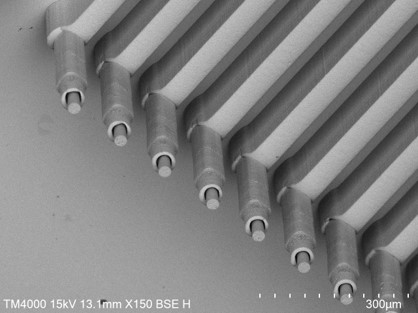
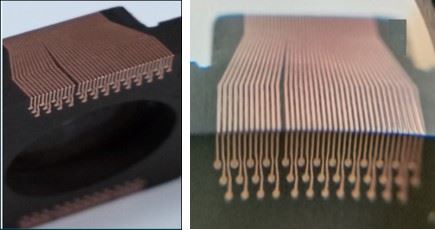
開發3D陶瓷電路板及微機電探針,取代環氧樹酯探針,探針精微化容易,提高一次測試晶粒數 (16 → 30或32)。結合微機電探針製程可發展模組化探針組裝技術,可將探針組裝由單根 / 次大幅提升百根 / 次以上,大幅減少組裝人力與成本。
3D ceramic circuit boards and MEMS probes have been developed to replace epoxy resin ring probes. The probes can reach fine pitch and increase testing grains (16 → 30 or 32) in one test. Combined with the MEMS probe process, modular probe assembly technology has been developed, which can massively increase the probe assembly efficiency from a single probe per time to more than one hundred probes at a time, greatly reducing assembly labor and cost.
特色與創新 Characters and Innovations
- 結合雷射圖案化與高選擇性金屬化技術,於3D陶瓷表 面製作 3D 金屬線路,具有低成本與高彈性優勢。
- 發展高硬度三元合金金屬化技術 (硬度≥800 HV),進行微機電探針製作。開發高精度積體化 3D 探針接合技術與雙面對準接合設備,進行模組化百根探針以上接合。
- Combining laser patterning and high-selective metallization technology, 3D metal circuits can be fabricated on the 3D ceramic surface, which has the advantages of low cost and high customization ability.
- High-hardness ternary alloy metallization technology (hardness ≥800 HV)has been developed and applied for the production of MEMS probes.
- High-precision integrated 3D probe bonding technology and double-sided alignment bonding equipment have been developed to achieve modular bonding of more than 100 probes.
應用與效益 Applications and Benefits
- 水平式探針卡、微機電探針、3D 陶瓷電路板。
- Horizontal probe card, MEMS probe, 3D ceramic circuit board.
聯絡 contact
- 張佑祥 Daniel Chang
- TEL:886-3-5912379
- FAX:886-3-5820043
- E-mail: yhchang@itri.org.tw
更多資訊

陶瓷3D電路板 3D Ceramic Circuit

三階MEMS探針 3D MEMS Probe